Manufacturing and Packaging

MCS recognises the importance of manufacturing and packaging technology towards managing the prohibitive costs of deploying large volumes of smart cards without compromising quality. This includes exploiting advanced process methodologies and packaging designs.  Many aspects are considered:

  • Card and inlay substrate material and design
  • IC module packaging design
  • Antenna design and coupling method
  • Roll- versus sheet-based production
  • Manual versus automated processes

To increase the marketability of smart cards in the future, we would like to introduce new card specifications and manufacturing processes which will bring down card production costs. As IC become more powerful and price come down, the card packaging costs will outstrip the cost of the IC!  For example, card dimensions do not matter in the case of contactless cards and smaller cards consume less material.  Case in point, Apple defied standards by mandating smaller SIM cards.

Furthermore, to address the consumer-driven market, the card must have a fresh, unique look, allows higher degree of personalisation and be easy to use. Departure from the standard look-and-feel would distinguish them from the old-fashioned cards being issued by various organizations.

Environment-friendly Paper Inlay

Secondly, on the medium issue, we looked at the use of ordinary paper of normal grammage ( 70 to 100 grams ) as the medium to house the silicon and the antenna. This then replaces the use of plastic and other plasticised materials like Teslin and other polycarbonate inlay materials. MCS collaborated with a machine manufacturer to produce greener contactless card inlays in an economical, high-volume process. To this end, in 2019, MCS successfully developed the “paper inlay” solution where the IC module and antenna are assembled on paper substrate which makes it extremely compatible with e-passport bookmaking process. Furthermore, the paper inlay is manufactured in a reel-to-reel process and may be produced in reel or sheet format. The reel format is advantageous for low-cost, high-volume manufacturing processes.

Paper Inlay Samples

Easy Conversion of Machine Readable Passport to E-Passport

Thin, flexible paper inlay with IC and antenna for conversion of machine readable passport to e-passport.

UniVisa

From the paper inlay, MCS developed the UniVisa electronic visa sticker that complies with ICAO Document 9303 Part 7 — Machine Readable Visas specifications.

The UniVisa incorporates an RFID chip and antenna which are embedded on security paper. It stores the bearer’s primary biodata including any biometric data such as face, iris and fingerprints. In essence, the UniVisa is similar (in logical data structures) to the ePassport with the exception that the medium used in the UniVisa is easily degradable.

UniVisa

The construction of the UniVisa comprises of a secure microcontroller with crypto processor coupled with a micro copper antenna, both of which are embedded onto the base security paper with a sticky laminate resulting in a true paper-based electronic visa suitable for countries that require visitors to be issued with visas. Ported onto the silicon device is the MCS Multi-application Operating System (MOS) that holds the ICAO recommended Visa logical data structures, customised to the host country’s Visa requirements.

Clearly the advantages are greater automation and increased security of immigration checks. To the travelers, eVisa is convenient. And, to the airlines, it enables quicker checks and reduced costs.

UniVisa Electronic Visa

UniVisa is a paper-based electronic visa compatible with ICAO Doc 9303 MRTD standard.

UniVisa e-Visa Enrolment and Inspection Demo

See a demonstration of the UniVisa e-Visa enrolment process at embassies and on-arrival. And inspection using standard passport reader and other wireless devices.

Smart Document

Smart Document

Another solution based on the paper inlay technology is an electronic seal which could be affixed to paper documents like birth certificates, university diplomas, work permits and so forth. As for the electronics, the smart RFID chip and its antenna are assembled on paper, designed like a seal or stamp, which is then laminated on to the security paper. There is no battery that needs to be maintained. If it was tampered with, the electronics will be rendered non-functional, also known as tamper-evident.


Nanomaterials

Keeping abreast of current technology is a necessity. Preparing for disruptive technologies of tomorrow is expected. MCS acknowledges the potential of nanotechnology in revolutionising the future semiconductor industry landscape and is pursuing the adoption of advanced materials within the manufacture and packaging of its products.

One such material is germanene. It is made up of one-atom thick layers formed from germanium, a semiconductor that was displaced by silicon. Researchers say that electrons conduct through germanium-based material ten times faster than through silicon and five times faster than in traditional germanium. So germanene beats silicon in electron conductivity and is not susceptible to oxidation. It also beats graphene in electronic applications because it has an inherent band gap and has 60 years of characterization for the electronics industry behind it. The old adage “what goes around comes around” is now being applied in electronics: silicon may be displaced by germanene in the near future.

Graphene

Another material is graphene, the thinnest material known – it consists of a single layer of carbon atoms and is both pliable and transparent. At the same time one of the strongest – it is 300 times stronger than steel. The material conducts electricity and heat very effectively. And perhaps most importantly, it is very inexpensive to produce.

In Malaysia, the National Graphene Action Plan 2020 was drafted as a result of an extensive collaboration between the Malaysian government, private sector companies, domestic and international research institutes, and academia to assess how Malaysia can benefit from the potential of Graphene. An explicit goal of the study was to determine Malaysia’s near-term action plan when innovating with Graphene.

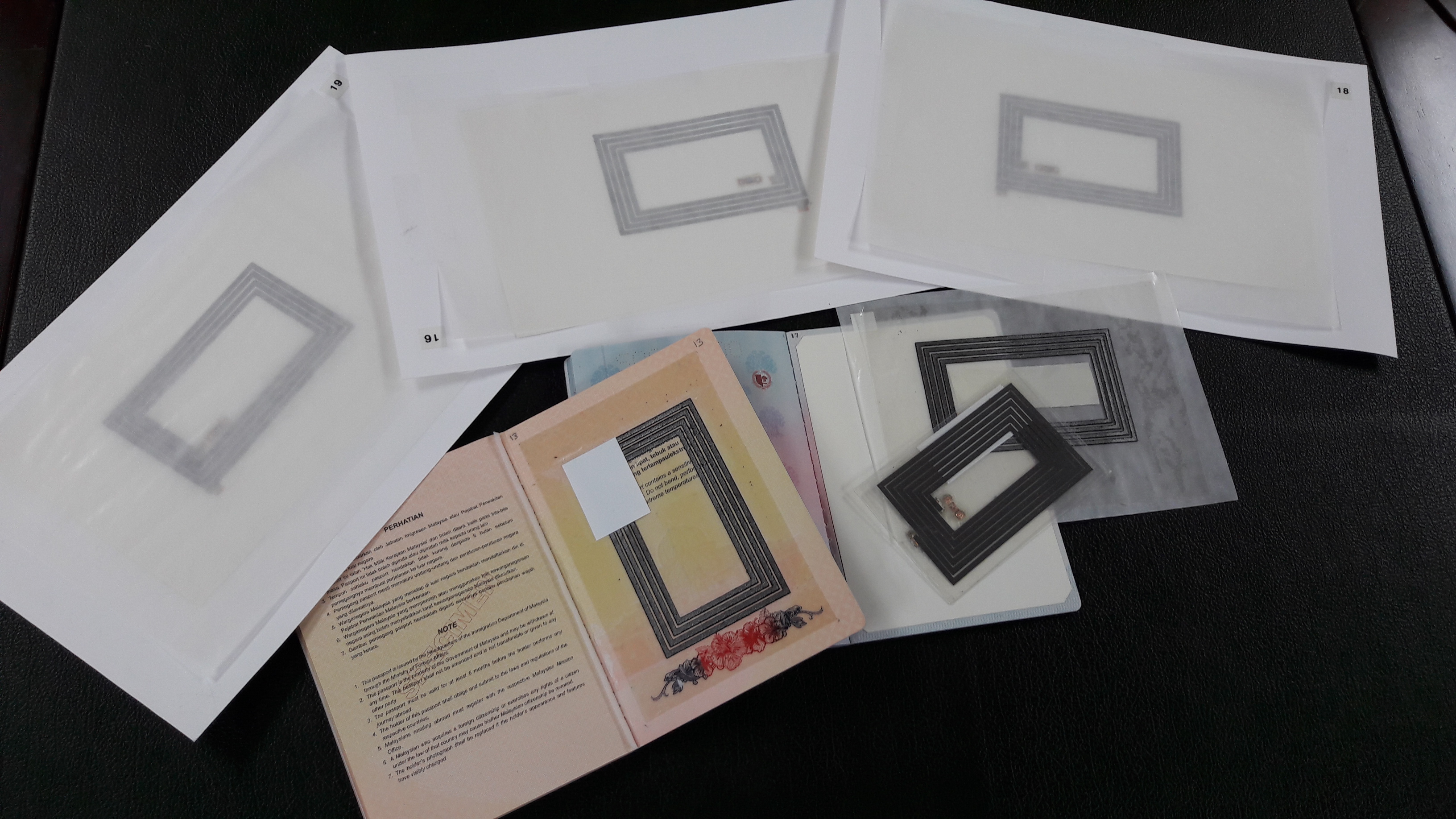
The NGAP2020 lays out a set of priority applications that will be beneficial to the country as a whole and what the government will do to support these efforts. One priority application is graphene-enabled conductive inks which provide a cost advantage (input and manufacturing) to radio frequency identification (RFID) applications, and eventually might be applicable to photovoltaics and printed circuits.

MCS hopes to translate its ambitions into reality and continue its legacy of creating products with leading edge technology. A prototype of the MCS e-passport with graphene antenna and MOS was showcased in the Mobile World Congress 2018 exhibition by the Italian research institute Consiglio Nazionale delle Ricerche (CNR), our technology partner. Next on our roadmap towards greener products is the technology to manufacture foldable, flexible, multi-layered printed circuit boards/layers (PCBs) made of graphene tracks on paper, plastic and other medium. And this, we believe is the next generation of electronics which will produce biodegradable products for the future.

Graphene antennae samples

Graphene Antenna on Paper Based Inlay with E-Passport

Graphene antenna on thin, flexible paper- or plastic-based inlay for e-passport and other ID applications.

Brochures

 TitleSize
UniVisa685.42 KB